
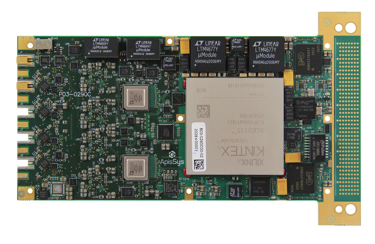
The AV129 is part of apissys’ range of High Speed data conversion and signal processing solutions based on the VITA 46, VPX standard.
The AV129 is fully compliant with OpenVPX standard, accommodating various communication protocols such as PCIe, SRIO, 1 Gbit and XAUI 10 Gbit Ethernet, as well as non OpenVPX adopted standard such as Aurora.
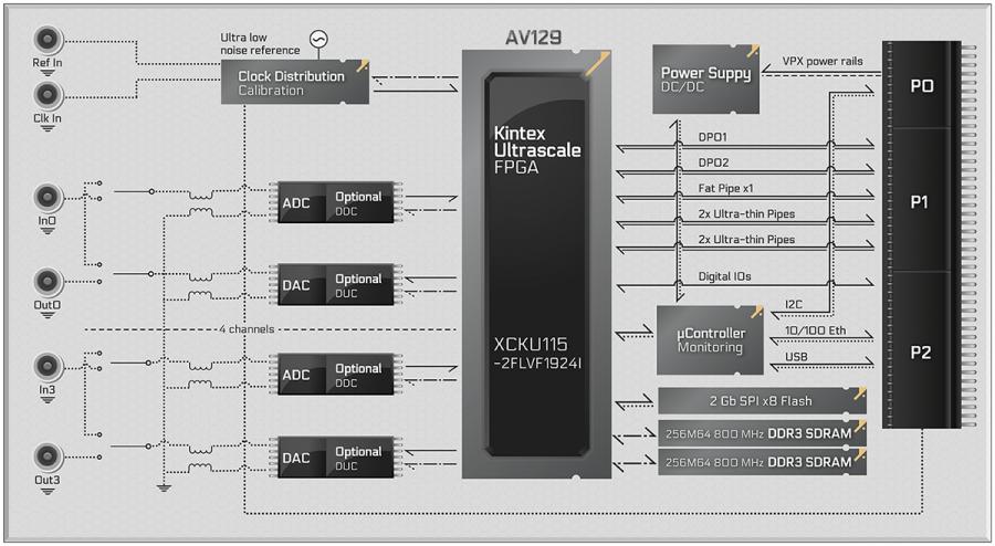
The AV129 combines four 14-bit 3 Gsps ADCs and four 16-bit 6/12 Gsps DAC with ultra-high processing power delivered by Xilinx® Kintex® Ultrascale™ FPGA, making it ideally suited for fully synchronous multiple channels test and measurement, MIMO, Electronic Warfare or Ultra-Wideband Radar Transceiver applications.
The AV129 features an internal ultra-low jitter reference and one clock synthesizer and can be used with either external clock or external reference for higher flexibility.
The AV129 includes one Xilinx® Kintex® Ultrascale™ KU115 FPGA for an impressive processing capability of more than 7 TMACs (Multiply Accumulate per second), two high speed 256M64 DDR3 SDRAM memory for data processing and two 1 Gb synchronous FLASH memory for multiple firmware storage.
The AV129 provides a USB 2.0 interface and a 10/100 Ethernet interface intended to be used for system monitoring and supervision.
The AV129 comes with complete software drivers for Windows and Linux. An FPGA Development Kit is provided including all necessary cores to build user FPGA application.
14-bit 3 Gsps Analog-Digital Converters
The AV129 Analog to Digital conversion is performed by two AD9208 dual channel 14-bit 3 Gsps ADCs with independent Digital Down Converters with decimation factor ranging from 2 to 48 in complex mode.The AV129 provides four front panel SMPM connectors for analog inputs. Single ended input signal are AC coupled with an input bandwidth from 2 GHz to 8 GHz with 6 dBm input level and up to X-Band with higher input level. A wideband signal generator is provided for on board, stand-alone calibration.
16-bit 6/12 Gsps Digital-Analog Converters
The AV129 Digital to Analog conversion is performed by four Analog Devices AD9162 16-bit 6/12 Gsps DACs with independent Digital Up Converters with interpolation factor ranging from 2 to 24 in complex mode.The AV129 provides four front panel SMPM connectors for analog outputs.Single ended output signals are AC coupled with an output bandwidth from 2 GHz to 7.5 GHz with 0 dBm output level. X-Band signals are supported with lower signal level.
Clock
The AV129 provides one ultra-low jitter clock synthesizer locked on a 100 MHz internal reference.The AV129 supports a 10 to 800 MHz external reference input either from a front panel SMPM connector or from the VPX P2 Connector.A reference output is available on VPX P2.External clock inputs for the ADCs are supported from either one SMPM connector or VPX P2. External clock from 2.5 GHz to 6 GHz are supported .
FPGA
The AV129 is fitted with a Xilinx® Kintex® Ultrascale™ KU115 user programmable FPGA. Only few resources are used to control and communicate with external hardware such as DDR3 SDRAM and monitoring sub-system, leaving most of the logic and block RAM and all DSP resources available for customer processing.Dedicated to signal processing, the Xilinx Kintex Ultrascale KU115 FPGA includes 1,451 K logics cells, 2,160 36 Kbit RAM blocs, 6 PCIe interface blocs and 5,520 DSP48 slices for an impressive processing power of more than 7 TMACs. The FPGA is delivered in -2 speed grade.
Dedicated to signal processing, the Xilinx Kintex Ultrascale KU115 FPGA includes 1,451 K logics cells, 2,160 36 Kbit RAM blocs, 6 PCIe interface blocs and 5,520 DSP48 slices for an impressive processing power of more than 7 TMACs.The FPGA is delivered in -2 speed grade.
Memories
The AV129 includes two 800 MHz 256M64 DDR3 SDRAM memory banks and two 1 Gbit QSPI FLASH used to store multiple FPGA configuration files.
VPX interface
The AV129 features an OpenVPX VITA 65 compliant interface with support for two Fat Pipes for Data Plane, one Fat Pipe for Expansion Plane, two Ultra-Thin Pipes for Control Plane and two User Defined Ultra-Thin Pipes on P1. The AV129 also supports 26 LVCMOS33 signals and 4 SUB-LVDS differential pairs on P2 plus USB2.0 and 10/100 Ethernet for supervision and monitoring.The AV129 features two low phase noise clock generators able to synthesize clock references for the FPGA GTHs from 60 MHz to 820 MHz, allowing support of all major protocols such as Aurora, GigE, PCIe Gen 1, 2 and 3, SATA, SRIO and XAUI 10Gbit Ethernet up to 16.375 Gbps.
Microcontroller
The AV129 features a 32-bit 80 MHz microcontroller used primarily for board monitoring and supervision.The microcontroller supports a USB 2.0 and a 10/100 Ethernet interfaces accessible on the VPX P2 user IO pins through an ApisSys AR102 Rear Transition Module or an ANSI/VITA 46.10 compliant custom RTM board.The microcontroller firmware includes all necessary features for board monitoring and supervision.
Firmware
The AV129 comes with a firmware package which includes VHDL cores allowing for control and communication with all AV129 hardware resources.A base design is provided which demonstrates the use of the AV129 and gives users a starting point for firmware development. The AV129 firmware package is supported on the Xilinx VIVADO® 2017.4 design suite and later.
Software
The AV129 is delivered with software drivers for Windows 10 and Linux.
Ruggedization
The AV129 is delivered in air cooled and conduction cooled standard or rugged versions for use in severe environmental conditions.Standard VITA 47 supported ruggedization levels are EAC4, EAC6, ECC3 and ECC4.
Analog Input / Output• Input Coupling: AC
• Input Full power bandwidth : 2 to 8 GHz • Input Full scale : 6 dBm • Output Coupling: AC • Output Full power bandwidth : 2 to 7.5 GHz • Output Full scale : 0 dBm • Impedance: 50 Ohm • Connectors: SMPM
|
Clock• Internal:
• One ultra-low jitter clock synthesizer • 2.5 GHz to 6.0 GHz low jitter clock • External Input Clock: • Frequency: 2.5 GHz to 6 GHz • Input level: 10 dBm recommended • Connector: SMPM, 50 Ohm and VPX P2 • External reference: • Frequency: 10 MHz to 800 MHz • Connector: SMPM, 50 Ohm and VPX P2
|
VPX interface• P1:
• Data plane: two fat pipes • Expansion plane: one fat pipe • Control plane: 2 ultra-thin pipes • 2 user-defined ultra-thin pipes • P2: • USB2.0 and 10/100 Ethernet • 28 LVCMOS33 signals • 4 SUB-LVDS differential pairs
|
| Part Number | A | V | 129 | - | rr | - | a | |
|---|---|---|---|---|---|---|---|---|
| Ruggedization level | Air Standard Air Rugged Conduction Standard Conduction Rugged |
- - - - |
- - - - |
- - - - |
- - - - |
AS AR CS CR |
- - - - |
- - - - |
| Options 1 | FPGA Kintex Ultrascale KU115 | - | - | - | - | - | - | 1 |
ECCN number: 3A002h1
| Air flow, Standard AS (VITA 47 EAC4 |
Air flow, Rugged AR (VITA 47 EAC6) |
Conduction Standard CS (VITA 47 ECC3) |
Conduction Rugged CR (VITA47 ECC4) |
|
|---|---|---|---|---|
| Operating Temperature |
0°C to +55°C (1) (8 CFM airfl ow at sea level) |
-40 to +70ºC (1) (8 CFM airfl ow at sea level) |
-40°C to +70°C (Card Edge) |
-40°C to +85°C (Card Edge) |
| Non Operating Temperature | -40°C to +85°C | -50°C to +100°C | -50°C to +100°C | -55°C to +105°C |
| Operating Vibration (Random) |
5Hz - 100Hz +3 dB/octave 100Hz-1kHz = 0.04 g2/Hz 1kHz - 2kHz -6 dB/octave |
5Hz - 100Hz +3 dB/octave 100Hz - 1kHz = 0.04 g2/Hz 1kHz - 2kHz -6 dB/octave |
5Hz - 100Hz +3 dB/octave 100Hz - 1kHz = 0.1 g2/Hz 1kHz - 2kHz -6 dB/octave |
5Hz - 100Hz +3 dB/octave 100Hz - 1kHz = 0.1 g2/Hz 1kHz - 2kHz -6 dB/octave |
| Operating Shock | 20g, 11 millisecond, half-sine | 20g, 11 millisecond, half-sine | 40g, 11 millisecond, half-sine | 40g, 11 millisecond, half-sine |
| Operating Relative Humidity |
0% to 95% non-condensing |
0% to 95% non-condensing |
0% to 95% non-condensing |
0% to 95% non-condensing |
| Operating Altitude |
@ 0 to 10,000 ft with adequate airflow |
@ 0 to 30,000 ft with adequate airflow |
@ 0 to 30,000 ft | @ 0 to 60,000 ft |
| Conformal Coating | No | Optional (default acrylic 1B31) | Yes (default acrylic 1B31) | Yes (default acrylic 1B31) |