
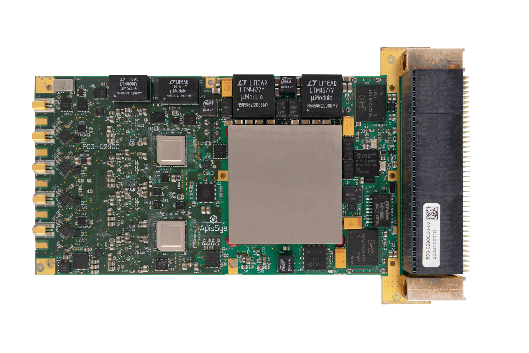
Presentation of the AV151 VPX board, for high resolution and ultra wideband applications
The AV151 is part of apissys’ range of Ultra Wideband Radar / ECM / SIGINT solutions based on the VITA47 ECC3, VPX standard.
Fully aligned with the SOSA standard, the AV151 supports a variety of communication protocols, including PCIe, Gigabit Ethernet and a large number of user-defined I/O. Additionally, the AV151 integrates key aspects of the OpenVPX standard, ensuring robust mechanical, electrical, and thermal interfaces. This hybrid approach makes the AV151 a versatile solution that leverages the best of both worlds, being compatible to both OpenVPX and SOSA, to provide enhanced interoperability and flexibility in demanding applications.
This VPX 3U board combines 4x 12-bit ADCs up to 20 Gsps, 4x 16-bit DACs up to 28 Gsps, and 18 GHz bandwidth with a Virtex® Ultrascale+™ FPGA, offering outstanding performance for demanding applications.
AMD Virtex® UltraScale+™ FPGAs offer the highest integration and performance capabilities in a 14 nm/16 nm FinFET node. These FPGAs offer the widest transceiver bandwidth, the highest number of DSPs, as well as the largest on-chip and in-package memory available in the UltraScale™ architecture. In addition, Virtex® UltraScale+™ FPGAs offer numerous power options to achieve an optimal balance between required system performance and the lowest energy envelope.
Target markets of this AV151 VPX board include Phased-Array Radar Transmitter / Receiver, Electronic Warfare ESM /ECM and Broadband Communication.
OpenVPX and the SOSA standard are two reference frameworks used for modular systems in the defense and aerospace industries. OpenVPX, based on the VPX standard, focuses on defining mechanical, electrical and thermal interfaces to ensure interoperability between modules from different suppliers. The SOSA (Sensor Open Systems Architecture) standard, on the other hand, goes a step further, integrating not only hardware interoperability aspects but also software specifications and communication protocols, thus promoting greater modularity and flexibility in the development of sensor and processing systems.
Our VPX card intelligently combines these two standards, leveraging the robustness and hardware interoperability of OpenVPX while incorporating the software and communication advances of the SOSA standard.
Equipped with 4 channels of 20 Gsps 12-bit ADC and 4 channels of 28 Gsps 16-bit DACs, the system offers a comprehensive solution for high-speed data acquisition and processing, including Direct Sampling capabilities.
Recent advancements in data converter technologies have led to a substantial increase in the sampling rate, opening up the potential to achieve a bandwidth of several tens of gigahertz for the most recent ADCs and DACs.
Many applications involving RF digitization use a method known as intermediate frequency (IF) sampling, where the analog signal is first converted to a lower intermediate frequency before being sampled by a converter.
Increasing sampling rates allow for direct sampling of the RF signal without the need for additional RF conversion stages, even for signals in the tens of gigahertz range. This approach, known as direct sampling, is now applicable to a wide range of radar and EW frequency bands, including the Ku, K, and Ka bands.
The RF direct sampling method can greatly simplify architectures and enhance the flexibility, scalability, and SWAP-C of equipment.
apissys, expert in wideband conversion solutions, is committed to designing products based on the latest technology to provide direct sampling capabilities for radar and electronic warfare applications.


Form Factor
VPX Profile
Analog Inputs/Outputs
Analog-Digital Conversion
Digital-Analog Conversion
Clock
Virtex Ultrascale+
Memory
Operating Temperature
Power dissipation (VU13P)
Weight
Board Support Package
VPX interface
P1:
-Data plane: one fat pipe DP01 supporting 100GBASE-KR4
-Data plane: one ultra-thin pipe DPutp01 supporting 10GBASE-KR
-Control plane: one ultra-thin pipe CPutp01 supporting 1000BASE-KX.
-Expansion plane: one fat-pipe supporting PCIE GEN3 4x
-Expansion plane: 8 LVDS differential pairs, configurable as 16 single ended LVCMOS
P2:
-Empty (SOSA-aligned profile)
or
-24 LVDS differential pairs, configurable as 48 single ended LVCMOS
| Part | Number | AV151 | c | a | b |
|---|---|---|---|---|---|
| FPGA | FPGA Virtex Ultrascale+ VU7P FPGA Virtex Ultrascale+ VU9P FPGA Virtex Ultrascale+ VU13P |
- - - |
- - - |
7 9 13 |
- - - |
| VPX P2 | Not fitted (SOSA-aligned) Fitted (48x User-defined IO extension) |
- - |
- - |
- - |
0 1 |
Availability: Rev.B June 2025
ECCN number: 3A002h1
| Environmental | Conduction-cooled Vita 47 class ECC3 |
| Operating Temperature | -40°C to +70°C (Card Edge) |
| Non Operating Temperature | -50°C to +100°C |
| Operating Vibration (Random) | 5Hz - 100Hz +3 dB/octave 100Hz - 1kHz = 0.01g2/Hz 1kHz - 2kHz -6 dB/octave |
| Operating Shock | 40g, 11 millisecond, half-sine |
| Operating Relative Humidity | 0% to 95% non-condensing |
| Operating Attitude | @ -1,500 to 60,000 ft |